 |
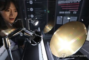
Photo: Hanmi Semiconductor |
[Alpha Biz= Kim Jisun] Hanmi Semiconductor is stepping up its push into the high-performance memory market with a new “two-in-one” bonding solution that enables two processes to be carried out on a single piece of equipment.
The company said on Feb. 27 that it has launched the world’s first BOC–COB bonder and will supply the system to a global memory customer’s manufacturing facility in Gujarat, India.
The new equipment integrates both the BOC (Board On Chip) and COB (Chip On Board) processes into a single platform—an industry first. Previously, semiconductor manufacturers were required to use separate dedicated tools for each process, leading to higher capital expenditures, larger factory footprints, and limited flexibility when product designs changed.
BOC, which relies on flip-chip bonding technology, is primarily used for DRAM applications requiring high-speed signal transmission. COB, a non-flip bonding process, is widely applied in high-capacity NAND flash memory. Demand for both processes is rising simultaneously in advanced memory segments such as stacked GDDR and enterprise SSDs used in AI semiconductors.
By enabling both processes on one machine, Hanmi’s new bonder enhances manufacturing flexibility, allowing customers to respond quickly to design changes without replacing equipment. It also improves space efficiency and reduces overall investment costs, prompting industry observers to view the product as a potential game changer in the memory back-end equipment market.
The system incorporates Hanmi’s proprietary TC bonder design expertise, particularly in precision thermal control—a critical factor for semiconductor yield. The company said advanced control systems were applied to both the chuck table and bonding head to ensure stable temperature management under diverse process conditions.
Hanmi Semiconductor has already established a strong position in the TC bonder market for high-bandwidth memory (HBM). It introduced its TC Bonder 4 for HBM4 last year and plans to launch a wide TC bonder targeting HBM5 and HBM6 processes in the second half of this year. The company is also expanding its AI packaging lineup with large-die FC bonders and TC bonders, aiming to broaden supply to foundries and outsourced semiconductor assembly and test (OSAT) providers.
Market conditions remain favorable. According to TrendForce, the global memory market is expected to grow 134% year-on-year to $551.6 billion in 2025, driven by rising AI server demand, followed by an additional 53% expansion to $842.7 billion in 2026.
Alphabiz Reporter Kim Jisun(stockmk2020@alphabiz.co.kr)