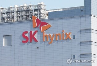
[Alpha Biz=(Chicago) Reporter Kim Jisun] SK Hynix will invest more than 1.3 trillion won in semiconductor cutting-edge packaging this year. Cutting-edge packaging is a process of stacking chips to increase performance or make different chips work like one chip.
Lee Kang-wook, vice president of P & T (Packaging & Test) at SK Hynix, said in an interview with Bloomberg News on the 7th, "We will invest more than $ 1 billion (about 1.33 trillion won) this year to improve cutting-edge packaging competitiveness." Lee is a former Samsung Electronics official and is considered a key executive who leads SK Hynix's cutting-edge packaging business.
One billion dollars is 10% of SK Hynix's investment estimate (about 13 trillion to 14 trillion won) this year. It is not uncommon to invest 10% of the investment only in state-of-the-art packaging, rather than the "pre-processing" process of making chips from wafers, which are disc of semiconductors. "The next 50 years in the semiconductor industry will be led by packaging," Lee said.
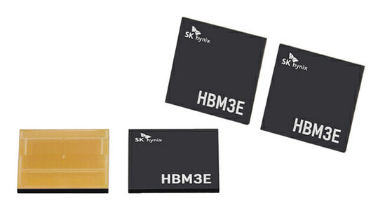
Behind SK Hynix's large-scale, state-of-the-art packaging investment is a fierce battle to preoccupy the HBM market.
Recently, memory semiconductor companies are competing to make high-capacity HBMs by stacking DRAMs in eight or 12 layers through state-of-the-art packaging.
Alphabiz Reporter Kim Jisun(stockmk2020@alphabiz.co.kr)